
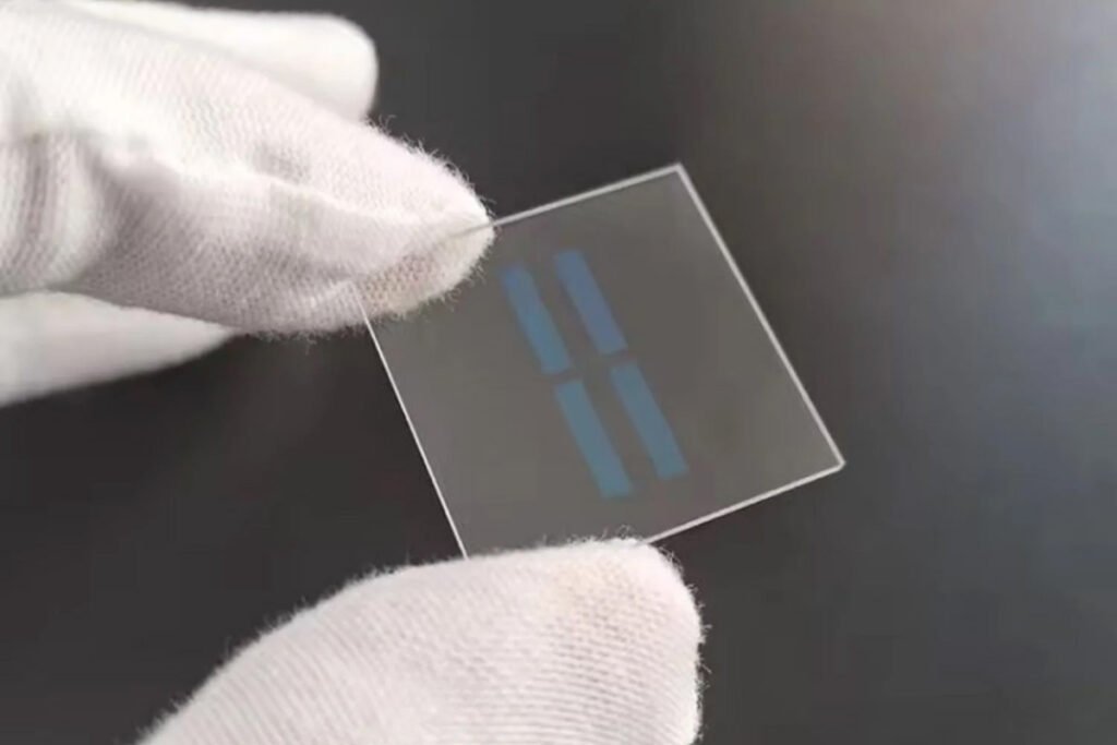
Transparent Electrode
Full-Surface ITO Glass
Continuous conductive film with defined edge exclusion and coated-side marking.
ITO coated glass combines optical transmission with electrical conductivity. The sheet-resistance value is only one part of the circuit: the actual resistance between contacts changes with the length-to-width ratio of the conductive path.
The coating side, electrode pattern, busbar material, contact method and thermal budget affect performance. A complete drawing identifies active and nonconductive zones, current direction, probe points and edge handling.
| Sheet resistance | Selected by electrical load and transmission trade-off; reference products span below 10 to 100+ ohms/square |
|---|---|
| Uniformity | Tolerance and sampling map agreed across the active area |
| Transmission | Spectrum or average value with substrate, thickness and coated side stated |
| Substrates | Soda-lime, borosilicate, alkali-free glass, thin glass or fused silica by request |
| Patterning | Full coat, isolated area or drawing-defined electrode pattern by feasibility review |
| Inspection | Four-point-probe sheet resistance plus optical and cosmetic checks |
Reference ranges are used for discussion only. The quotation identifies the controlled values and inspection method.
Use the calculator to understand the first-order relationship. Final designs require busbar, contact and temperature analysis.
Estimated path resistance R = sheet resistance x L / W
Geometry estimate only. Contacts, busbars, patterning, temperature and film uniformity affect the real circuit.
Each configuration changes the electrical path, optical requirement and downstream handling.
Continuous conductive film with defined edge exclusion and coated-side marking.
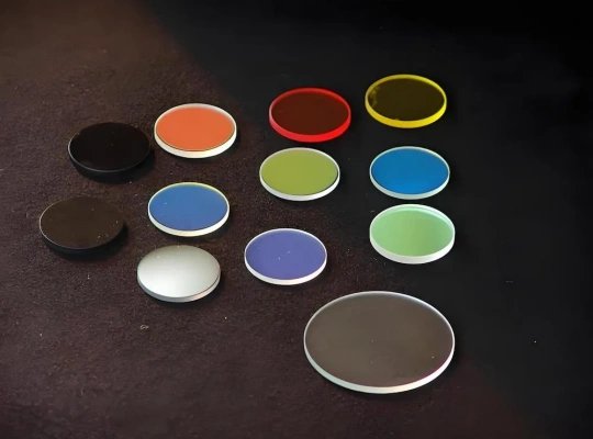
Drawing-defined active and isolated areas for sensors, cells or research devices.
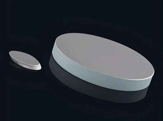
Conductive path and busbars designed around voltage, power density and uniformity.
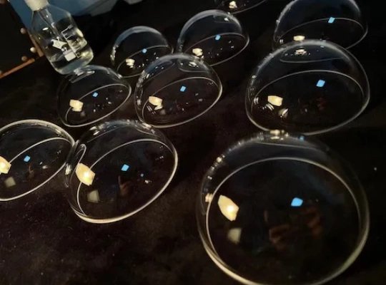
Alternate substrates for temperature, chemistry or spectral requirements.
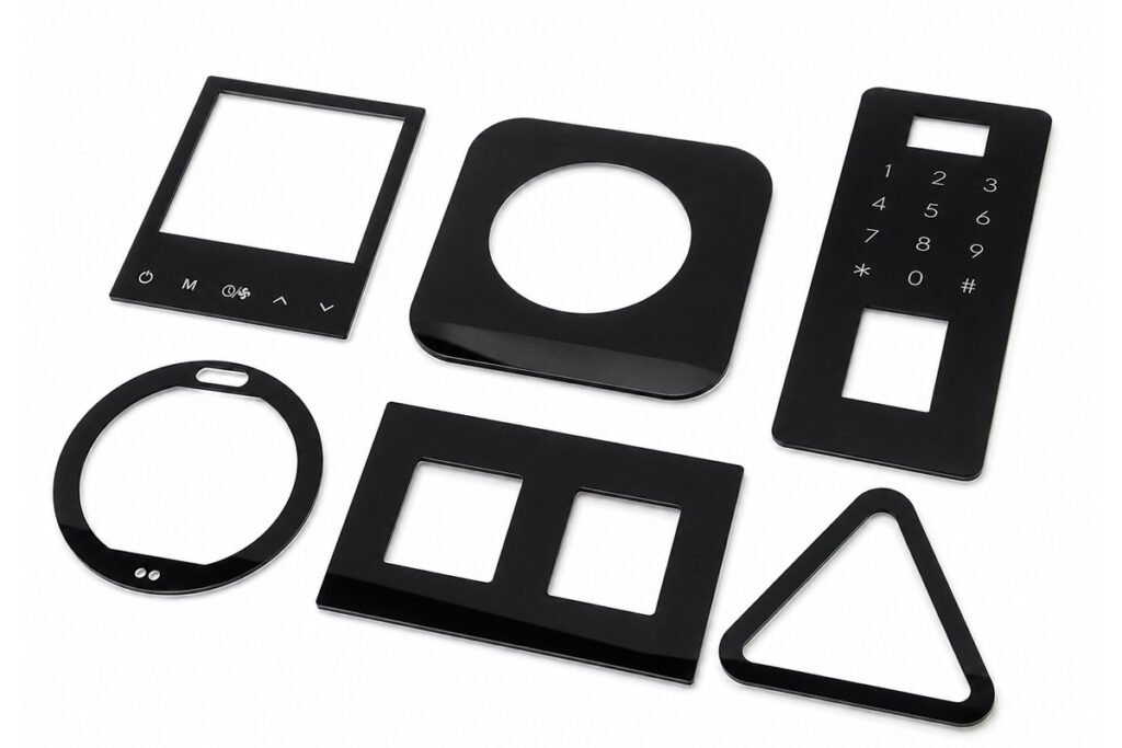
Independent conductive surfaces requiring side identification and isolation review.
For a uniform thin film, a square measured from one opposite edge to the other has the same resistance whether the square is 10 mm or 100 mm wide. A longer rectangle contains more squares in series; a wider path places more squares in parallel. The first-order relation is R = Rs x L/W. Real devices add contact resistance, nonuniformity, temperature coefficient, patterned geometry and busbar effects.
ITO films can be optically clear yet electrically discontinuous, or electrically acceptable with visible defects. Both data sets are required.
Lock substrate, coating side, optical or electrical target, test method and downstream process.
Complete cutting, CNC, edge work, cleaning and any compatible strengthening before the controlled coating step.
Apply the selected etch or coating route with orientation, masking and handling controls.
Measure the page-specific optical, surface or electrical characteristics and record uniformity.
Inspect controlled zones and protect the functional surface against contact and contamination.
Inspection conditions and acceptance limits are linked to the approved drawing and coating specification.
Share the circuit, not only the glass dimensions.
It depends on voltage, path geometry, current, power density and acceptable optical loss. Start with the electrical design rather than a generic grade.
A four-point probe is commonly used because it separates the film measurement from lead/contact resistance. Define the sampling grid and tolerance.
Often a conductivity/transmission trade-off exists because film thickness and carrier properties affect both. Review actual spectral data for the selected construction.
Selected coated stock can be fabricated, but coated-side protection, edge damage, contamination and post-process continuity must be controlled.
Drawing-defined patterns can be reviewed. Provide line widths, isolation gaps, registration, active area and electrical test points.
Yes for suitable resistance, geometry, busbars, voltage and control design. Thermal simulation and assembled testing are required.
Include: Substrate, thickness and outside dimensions | Sheet resistance and uniformity target | Transmission wavelength/band | Coated side and active-area drawing | Pattern, busbar and contact details | Voltage/current or device function | Downstream heat and chemical exposure.
The active area, busbars and probe points should use the same datums as the glass outline. The review identifies the proposed substrate, coating route, measurement method, sample plan and open technical points.
Tell us the material, size, thickness, tolerance, quantity, application, and any holes, slots, edges, coating, printing, or polishing requirements. We can manufacture custom glass components from your drawing, CAD file, sketch, or sample.